- 您现在的位置:买卖IC网 > Sheet目录3831 > PIC18F4423-I/ML (Microchip Technology)IC PIC MCU FLASH 8KX16 44QFN
PIC18F2423/2523/4423/4523
DS39755C-page 34
2009 Microchip Technology Inc.
2.8
Use of the CCP2 Trigger
An A/D conversion can be started by the Special Event
Trigger of the CCP2 module. This requires that the
CCP2M<3:0> bits (CCP2CON<3:0>) be programmed
as ‘1011’ and that the A/D module is enabled (ADON
bit is set). When the trigger occurs, the GO/DONE bit
will be set, starting the A/D acquisition and conversion,
and the Timer1 (or Timer3) counter will be reset to zero.
Timer1 (or Timer3) is reset to automatically repeat the
A/D acquisition period with minimal software overhead
(moving ADRESH:ADRESL to the desired location).
The appropriate analog input channel must be selected
and the minimum acquisition period is either timed by
the user or an appropriate TACQ time is selected before
the Special Event Trigger sets the GO/DONE bit (starts
a conversion).
If the A/D module is not enabled (ADON is cleared), the
Special Event Trigger will be ignored by the A/D
module, but will still reset the Timer1 (or Timer3)
counter.
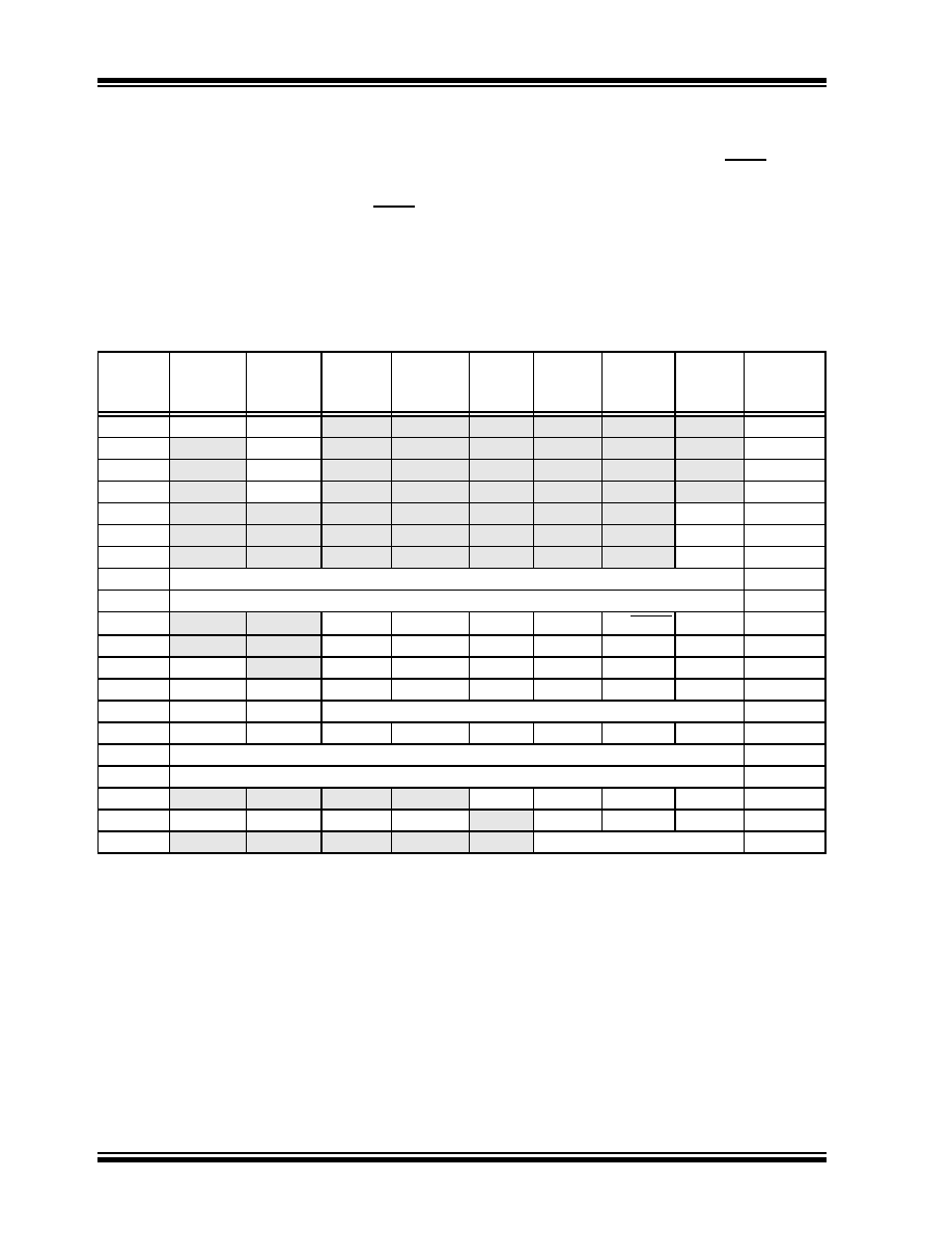
TABLE 2-3:
REGISTERS ASSOCIATED WITH A/D OPERATION
Name
Bit 7
Bit 6
Bit 5
Bit 4
Bit 3
Bit 2
Bit 1
Bit 0
Reset
Values on
page
INTCON
GIE/GIEH PEIE/GIEL TMR0IE
INT0IE
RBIE
TMR0IF
INT0IF
RBIF
(Note 4)
PIR1
PSPIF(1)
ADIF
RCIF
TXIF
SSPIF
CCP1IF
TMR2IF
TMR1IF
(Note 4)
PIE1
PSPIE(1)
ADIE
RCIE
TXIE
SSPIE
CCP1IE
TMR2IE
TMR1IE
(Note 4)
IPR1
PSPIP(1)
ADIP
RCIP
TXIP
SSPIP
CCP1IP
TMR2IP
TMR1IP
(Note 4)
PIR2
OSCFIF
CMIF
—
EEIF
BCLIF
HLVDIF
TMR3IF
CCP2IF
(Note 4)
PIE2
OSCFIE
CMIE
—
EEIE
BCLIE
HLVDIE
TMR3IE
CCP2IE
(Note 4)
IPR2
OSCFIP
CMIP
—
EEIP
BCLIP
HLVDIP
TMR3IP
CCP2IP
(Note 4)
ADRESH
A/D Result Register High Byte
(Note 4)
ADRESL
A/D Result Register Low Byte
(Note 4)
ADCON0
—
CHS3
CHS2
CHS1
CHS0
GO/DONE
ADON
(Note 4)
ADCON1
—
VCFG1
VCFG0
PCFG3
PCFG2
PCFG1
PCFG0
(Note 4)
ADCON2
ADFM
—
ACQT2
ACQT1
ACQT0
ADCS2
ADCS1
ADCS0
(Note 4)
PORTA
RA7(2)
RA6(2)
RA5
RA4
RA3
RA2
RA1
RA0
(Note 4)
TRISA
TRISA7(2) TRISA6(2) PORTA Data Direction Control Register
(Note 4)
PORTB
RB7
RB6
RB5
RB4
RB3
RB2
RB1
RB0
(Note 4)
TRISB
PORTB Data Direction Control Register
(Note 4)
LATB
PORTB Data Latch Register (Read and Write to Data Latch)
(Note 4)
PORTE(1)
—
—RE3(3)
RE2
RE1
RE0
(Note 4)
TRISE(1)
IBF
OBF
IBOV
PSPMODE
—
TRISE2
TRISE1
TRISE0
(Note 4)
LATE(1)
—
PORTE Data Latch Register
(Note 4)
Legend: — = unimplemented, read as ‘0’. Shaded cells are not used for A/D conversion.
Note 1: These registers and/or bits are not implemented on PIC18F2423/2523 devices and are read as ‘0’.
2: PORTA<7:6> and their direction bits are individually configured as port pins based on various primary
oscillator modes. When disabled, these bits read as ‘0’.
3: RE3 port bit is available only as an input pin when the MCLRE Configuration bit is ‘0’.
4: For these Reset values, see Section 4.0 “Reset” of the “PIC18F2420/2520/4420/4520 Data Sheet”
(DS39631).
发布紧急采购,3分钟左右您将得到回复。
相关PDF资料
PIC16F874A-I/P
IC MCU FLASH 4KX14 EE 40DIP
PIC18F87J60-I/PT
IC PIC MCU FLASH 64KX16 80TQFP
PIC24HJ128GP202-I/MM
IC PIC MCU FLASH 128K 28-QFN
PIC16F873-04/SO
IC MCU FLASH 4KX14 EE 28SOIC
PIC24FJ128GA106-I/PT
IC PIC MCU FLASH 64TQFP
AT87C51RD2-RLTUM
IC 8051 MCU 64K OTP 40MHZ 44VQFP
AT87C51RD2-RLTUL
IC 8051 MCU 64K OTP 30MHZ 44VQFP
PIC16F873-04/SP
IC MCU FLASH 4KX14 EE 28DIP
相关代理商/技术参数
PIC18F4423-I/P
功能描述:8位微控制器 -MCU 16KB 768bytes-RAM 36I/O RoHS:否 制造商:Silicon Labs 核心:8051 处理器系列:C8051F39x 数据总线宽度:8 bit 最大时钟频率:50 MHz 程序存储器大小:16 KB 数据 RAM 大小:1 KB 片上 ADC:Yes 工作电源电压:1.8 V to 3.6 V 工作温度范围:- 40 C to + 105 C 封装 / 箱体:QFN-20 安装风格:SMD/SMT
PIC18F4423-I/PT
功能描述:8位微控制器 -MCU 16KB 768bytes-RAM 36I/O RoHS:否 制造商:Silicon Labs 核心:8051 处理器系列:C8051F39x 数据总线宽度:8 bit 最大时钟频率:50 MHz 程序存储器大小:16 KB 数据 RAM 大小:1 KB 片上 ADC:Yes 工作电源电压:1.8 V to 3.6 V 工作温度范围:- 40 C to + 105 C 封装 / 箱体:QFN-20 安装风格:SMD/SMT
PIC18F4423-I/PT
制造商:Microchip Technology Inc 功能描述:8-Bit Microcontroller IC
PIC18F4423T-I/ML
功能描述:8位微控制器 -MCU 16KB 768bytes-RAM 36I/O RoHS:否 制造商:Silicon Labs 核心:8051 处理器系列:C8051F39x 数据总线宽度:8 bit 最大时钟频率:50 MHz 程序存储器大小:16 KB 数据 RAM 大小:1 KB 片上 ADC:Yes 工作电源电压:1.8 V to 3.6 V 工作温度范围:- 40 C to + 105 C 封装 / 箱体:QFN-20 安装风格:SMD/SMT
PIC18F4423T-I/PT
功能描述:8位微控制器 -MCU 16KB 768bytes-RAM 36I/O RoHS:否 制造商:Silicon Labs 核心:8051 处理器系列:C8051F39x 数据总线宽度:8 bit 最大时钟频率:50 MHz 程序存储器大小:16 KB 数据 RAM 大小:1 KB 片上 ADC:Yes 工作电源电压:1.8 V to 3.6 V 工作温度范围:- 40 C to + 105 C 封装 / 箱体:QFN-20 安装风格:SMD/SMT
PIC18F442-E/L
功能描述:8位微控制器 -MCU 16KB 768 RAM 34I/O RoHS:否 制造商:Silicon Labs 核心:8051 处理器系列:C8051F39x 数据总线宽度:8 bit 最大时钟频率:50 MHz 程序存储器大小:16 KB 数据 RAM 大小:1 KB 片上 ADC:Yes 工作电源电压:1.8 V to 3.6 V 工作温度范围:- 40 C to + 105 C 封装 / 箱体:QFN-20 安装风格:SMD/SMT
PIC18F442-E/ML
功能描述:8位微控制器 -MCU 16KB 768 RAM 34I/O RoHS:否 制造商:Silicon Labs 核心:8051 处理器系列:C8051F39x 数据总线宽度:8 bit 最大时钟频率:50 MHz 程序存储器大小:16 KB 数据 RAM 大小:1 KB 片上 ADC:Yes 工作电源电压:1.8 V to 3.6 V 工作温度范围:- 40 C to + 105 C 封装 / 箱体:QFN-20 安装风格:SMD/SMT
PIC18F442-E/P
功能描述:8位微控制器 -MCU 16KB 768 RAM 34I/O RoHS:否 制造商:Silicon Labs 核心:8051 处理器系列:C8051F39x 数据总线宽度:8 bit 最大时钟频率:50 MHz 程序存储器大小:16 KB 数据 RAM 大小:1 KB 片上 ADC:Yes 工作电源电压:1.8 V to 3.6 V 工作温度范围:- 40 C to + 105 C 封装 / 箱体:QFN-20 安装风格:SMD/SMT